混合鹵素CsPbBrxI3–x鈣鈦礦量子點(diǎn)具有良好光譜可調(diào)性,在純紅光鈣鈦礦發(fā)光二極管領(lǐng)域中具有良好的應(yīng)用潛力。然后,該類(lèi)量子點(diǎn)面臨著表面缺陷和不穩(wěn)定性這兩大難題,嚴(yán)重阻礙了其在高性能器件中的實(shí)際應(yīng)用價(jià)值。
基于此,鄭州大學(xué)張繼斌研究員與華中科技大學(xué)屠國(guó)力教授等人報(bào)道了采用釔陽(yáng)離子(Y3+)摻雜和苯基膦酸(PPA)鈍化的協(xié)同策略來(lái)解決這些問(wèn)題。其中,引入Y3+離子摻雜后,量子點(diǎn)的形成能得以降低,而碘化物空位缺陷的形成能則有所增加。PPA則通過(guò)其膦氧化物基團(tuán)與未配位的 Pb2+離子配位,成功實(shí)現(xiàn)了對(duì)表面缺陷的有效鈍化。并且,PPA的羥基還能與相鄰鹵素離子形成氫鍵,抑制了鹵素離子的遷移,進(jìn)一步增強(qiáng)了鈍化效果。
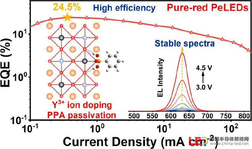
最終,Y/PPA 共改性量子點(diǎn)表現(xiàn)出了卓越的穩(wěn)定性,光致發(fā)光量子產(chǎn)率近乎達(dá)到100%。基于這些量子點(diǎn)的鈣鈦礦發(fā)光二極管具有出色的光譜穩(wěn)定性,外量子效率達(dá)到24.5%,是基于 CsPbBrxI3–x量子點(diǎn)的純紅光鈣鈦礦發(fā)光二極管效率最高者之一。
該工作得到了國(guó)家重點(diǎn)研發(fā)計(jì)劃、國(guó)家自然科學(xué)基金、中國(guó)博士后科學(xué)基金等項(xiàng)目資助。
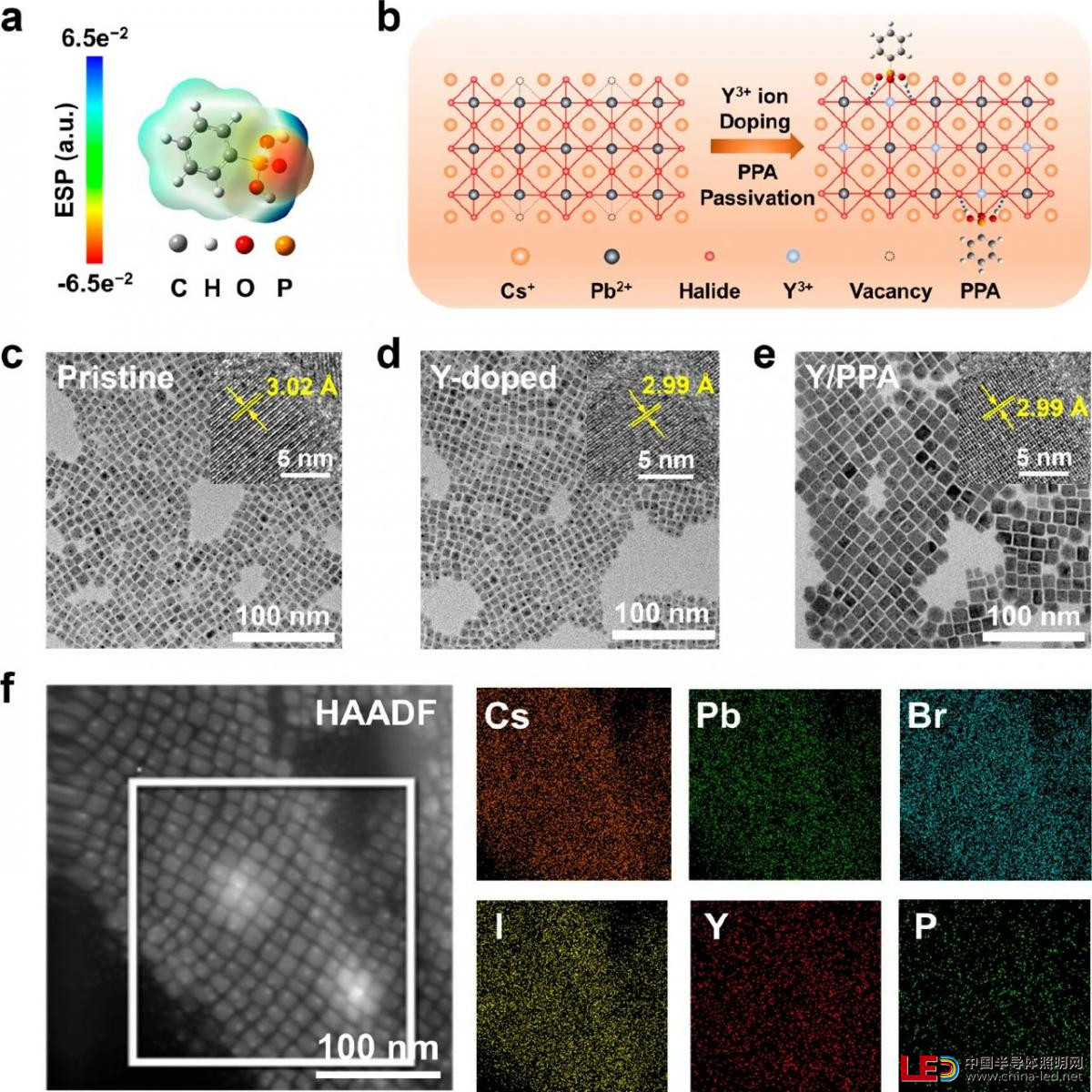
Figure 1. (a) Electrostatic potential (ESP) map of PPA molecules. (b) Schematic illustration of CsPbBrxI3-xNCs before and after synergistic modification of Y3+ ion doping and PPA passivation. TEM images of (c) pristine, (d) Y-doped, and (e) Y/PPA NCs. The insets show corresponding HRTEM images. (f) Elemental mapping images of Y/PPA NCs.
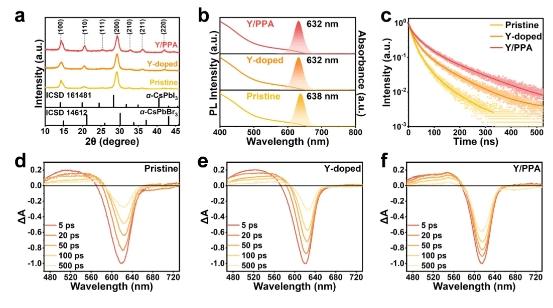
Figure 2. (a) XRD patterns, (b) PL and Absorption spectra, (c) Time-resolved PL decay curves of pristine, Y-doped, and Y/PPA NCs. TA spectra of (d) pristine, (e) Y-doped, and (f) Y/PPA NCs at different probe delay times.
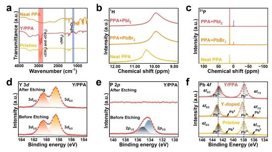
Figure 3. (a) FTIR spectra of pristine NCs, Y/PPA NCs, and neat PPA. (b) 1H and (c) 31P NMR spectra of neat PPA, a mixture of PPA and PbBr2, and a mixture of PPA and PbI2 in dimethyl sulfoxide (DMSO-d6) solution. High-resolution XPS spectra of (d) Y 3dand (e) P 2p of Y/PPA NCs before etching and after etching. (f) High-resolution XPS spectra of Pb 4f of pristine, Y-doped, and Y/PPA NCs.
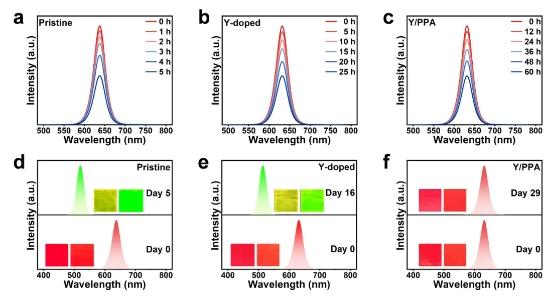
Figure 4. PL spectra of (a) pristine, (b) Y-doped, and (c) Y/PPA NC films at different times (photostability test: under UV light continuous irradiation). (d) PL spectra of pristine NC films on day 0 and day 5 (stability test: 40 ℃ and 80% RH). The insets show the corresponding photographs of pristine NC films under daylight (left) and UV light (right) on day 0 and day 5. (e) PL spectra of Y-doped NC films on day 0 and day 16 (stability test: 40 ℃ and 80% RH). The insets show the corresponding photographs of Y-doped NC films under daylight (left) and UV light (right) on day 0 and day 16. (f) PL spectra of Y/PPA NC films on day 0 and day 29 (stability test: 40 ℃ and 80% RH). The insets show the corresponding photographs of Y/PPA NC films under daylight (left) and UV light (right) on day 0 and day 29.
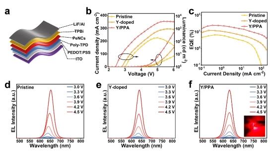
Figure 5. (a) Device structure of PeLEDs. (b) Current density−voltage−luminance curves of PeLEDs. (c) EQE−current density curves of PeLEDs. EL spectra of PeLEDs based on (d) pristine, (e) Y-doped, and (f) Y/PPA NCs at different bias voltages. The inset shows a working PeLED.
